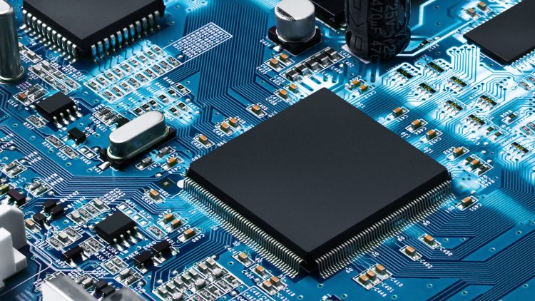
50% Incentives for all semiconductor fabs by Govt of India
Cabinet adopts changes to "India's Semiconductor and Display Manufacturing Ecosystem" Offer 50% incentives for semiconductor fabs across technological nodes, compound semiconductors, packaging, and other facilities.
Authorised the following changes to India's semiconductor and display production programme:
The amendments detailed below were authorised by the Cabinet, which is led by the Prime Minister and is presided over by Shri Narendra Modi. The modifications were made to the Programme for the Development of the Semiconductor and Display Manufacturing Ecosystem in India.
Under the Scheme for Setting up Semiconductor Fabs in India
The government will provide financial assistance equal to 50 percent of the total cost of the project on a per-technology basis.
A fiscal support of fifty percent of the project cost on a per-unit basis, as allotted by the Scheme for Establishing Display Fabs.
Under the Scheme for Setting up of Compound Semiconductors / Silicon Photonics / Sensors Fab and Semiconductor ATMP /OSAT facilities in India, the government will provide financial support equal to fifty percent of the total capital expenditures on a pari-passu basis. In addition, Discrete Semiconductor Fabs will be included as one of the target technologies under the Scheme.
For the purpose of establishing semiconductor fabrication facilities, a modified programme will offer a consistent level of financial assistance equal to fifty percent of the total cost of the project. In light of the specialised nature of compound semiconductors and advanced packaging, the modified programme will also offer financial support of up to fifty percent of capital expenditures on a pari-passu basis for the establishment of fabs that produce silicon photonics, sensors, compound semiconductors, and discrete semiconductors. This support will be provided for ATMP/OSAT and compound semiconductors.
Many major semiconductor firms have expressed interest in establishing fabs in India as a result of the scheme. The revised programme would hasten the pace at which investments are made in India's semiconductor and display manufacturing industries. On the basis of the conversations that have taken place with prospective investors, it is anticipated that the process of constructing the first semiconductor facility will start very soon.
In order to provide guidance to India Semiconductor Mission, the nodal agency for the Programme for Development of India's Semiconductor and Display Manufacturing Ecosystem, an Advisory Committee made up of global experts from industry and academia was established. The mission's goal is to create an ecosystem in India that is conducive to the production of semiconductors and displays. The Government has decided to follow the advice of the Advisory Committee and provide uniform support for all technology nodes of silicon semiconductor fabs, Silicon Photonics, Sensors, Discrete Semiconductor Fabs, and ATMP/OSAT. This recommendation was made by the committee unanimously. The demand for technology nodes 45nm and beyond is significant, and it is being driven in part by applications in the automotive, power, and telecommunications industries. In addition to that, this submarket accounts for approximately half of the total semiconductor market.
What's Your Reaction?